
Just because we can’t see something doesn’t mean it’s not there. A lot is hidden to the naked eye – molecular structures, for example. We have only been able to gain an insight into these, the smallest of structures, since microscopes were invented. Sometimes, the images researchers see through a microscope could almost be classed as modern art.
Controlled dewetting
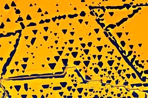
This image taken using a scanning electron microscope shows a gold film which is only 20 nanometres thick, approximately one thousand times thinner than a human hair. (Image: Peter Schweizer)
This image taken using a scanning electron microscope shows a gold film which is only 20 nanometres thick, approximately one thousand times thinner than a human hair. Using a process known as sputtering, the gold was bombarded with high-energy ions and deposited on a layer of molybdenum disulphide (MoS2). MoS2 is a graphite-like substance which is predominantly used in industry as a dry lubricant. ‘Molybdenum disulphide is highly interesting for our research, as, like graphene, it acts as a two dimensional carrier and bonds very well to metals,’ explains Peter Schweizer from the Chair of Micro- and Nanostructure Research.
If the gold is heated after sputtering, it adjusts to the crystal structure of the molybdenum disulphide and forms an even film from approximately 500 °C. If the temperature increases further, however, a dewetting process is set in motion even before the melting point of gold is reached. This effect, which intensifies the thinner the film is, poses a problem for microelectronics, as it can lead to contact points becoming unattached, which can in turn lead to the failure of entire components. However, the process known as ‘solid state dewetting’, can also be used to fabricate nanoparticles on the basis of substrates, the size, shape and sequence of which can be controlled using various parameters.
The microscope image shows the typical triangles formed by the gold at the start of the dewetting process as it adjusts to the crystal structure of the carrier material. By increasing the temperature during a controlled procedure, the researchers led by EAM Member Prof. Dr. Erdmann Spiecker were able to gradually extend the size of the holes until a thin network of gold filaments was left. The process, known as ‘templated dewetting’, may be able to be used in future to create metal meshes which can act as conductors in spite of being transparent. Such transparent conductors are of interest, for example, for photovoltaic applications, as they could be used to increase the usable light absorption area of solar modules, and thereby their efficiency.
A clever combination
The image was taken using the FEI Helios Nanolab 660 scanning electron microscope at the Center for Nanoanalysis and Electron Microscopy at FAU. This piece of equipment uses a combination of scanning electron microscopy and a focused ion beam (FIB) and eight different detectors to provide high-resolution images from a wide range of signals such as secondary electrons, X-rays and secondary ions.
Stars on the horizon
The image shows a two dimensional carbon lattice. The star-shaped rings, approximately three nanometres in size, each consist of six triangular molecules, which in turn consist of 21 carbon atoms, three oxygen atoms and one nitrogen atom. The structure is the result of a bonding process taking place in several stages: Carbon molecules are vaporised in a vacuum chamber and attach to a gold film which acts as a catalyst. When heated to approximately 280°C, the molecules bond to each other of their own accord, firstly in one dimensional chains, then in a two-dimensional network.
In the collaborative research centre SFB 953 ‘Synthetic carbon allotropes’, researchers are investigating the electronic, optic, thermal and mechanic properties of carbon allotropes such as these. As carbon is capable of bonding almost without restriction to itself and to nearly every other element, it is the ideal material to use for tailored synthesis to diverse components with a wide range of functions which can then be used in nanoelectronics, photovoltaics, in sensors, batteries or super condensers. ‘Carbon allotropes can open up entirely new horizons where silicon technology reaches its limits with respect to scalability and efficiency,’ says EAM Professor Sabine Maier, who holds the Professorship for Scanning Probe Microscopy at FAU.
As an experimental physicist, Maier focuses on analysing the atomic structure and band gaps of 2D carbon lattices. A band gap is a type of barrier between the energy bands in solid objects which can be crossed when electrons get excited and is therefore a decisive criterion for using semiconductors in electronic components. Prof. Maier uses a scanning probe microscope in a vacuum at minus 268°C to probe the molecule lattice, allowing her to determine the topography of the sample down to the level of individual atoms. ‘We were first able to prove that the band gap diminishes as dimensionality increases in the case of covalent-bonded organic molecular structures on metallic surfaces,’ says Maier.
Precise
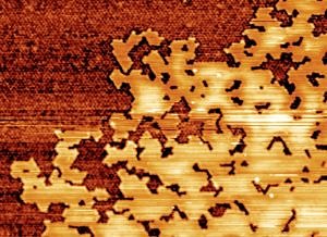
Unlike light microscopy, where the image is created by lenses, scanning electron microscopy creates the image as a result of interaction between a probe and a sample. The probe scans the surface of the sample and the measurements of the individual points on the sample are then compiled to give a digital image.
Goldsponge in CT
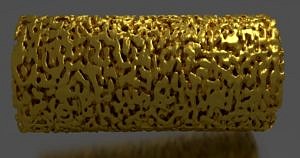
This cylindrical gold sponge has a diameter of only a few micrometres. In order to produce the porous network, an alloy of gold and silver is treated initially with nitric acid, which causes the silver atoms to detach selectively. Thereafter, the size of the ligaments in the structure can be adjusted using heat treatment and is approximately 300 nanometres in the example shown. The image is the result of a 3D analysis using high resolution x-ray tomography. The sample is bombarded with rays from all sides, similar to a CT image in medical applications. Special reconstruction algorithms followed by a rendering process create a three-dimensional image from the two-dimensional tomography data.
The research training group GRK 1896 ‘In situ microscopy with electrons, x-rays and scanning probes’ is investigating the mechanical properties of such openly porous materials derived from alloys. Gold sponge samples with various structures are observed under the microscope whilst being subjected to mechanical pressure. The equipment used includes the nano-CT mentioned above as well as a transmission electron microscope. ‘We were able to observe the deformation of the sample directly at the atomic level,’ explains Dr. Benjamin Apeleo Zubiri, a researcher at the Chair of Micro- and Nanostructure Research. ‘In combination with tomographical methods and correlative simulations, we were also able to discover to what extent parameters such as the size of the ligaments, the network architecture or special crystal defects impact the solidity or elasticity of the samples.’
Nanostructured networks are of interest for a wide range of applications: Metal sponges can form the basis of ultralight components with special damping properties. Their special properties such as simple adjustment of ligament size and the large internal surface area mean that they have great potential for use as catalyst materials, as electrochemical sensors or as electrodes in fuel cells.
X-ray vision
The image was taken using the ZEISS Xradia 810 Ultra X-ray microscope at the CENEM at FAU. This high resolution microscope worth 3.1 million euros allows researchers to conduct non-destructive analyses of the 3D structure of complex materials on a sub-micrometre scale and use the valuable information obtained for the targeted development of new materials.
About the author
Matthias Münch studied sociology before working as a freelance journalist for several daily newspapers. Since 2001, he has been providing support for companies and academic institutions in the areas of PR and corporate communication.